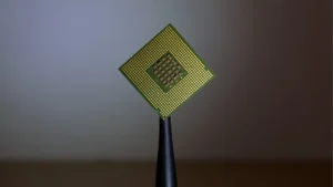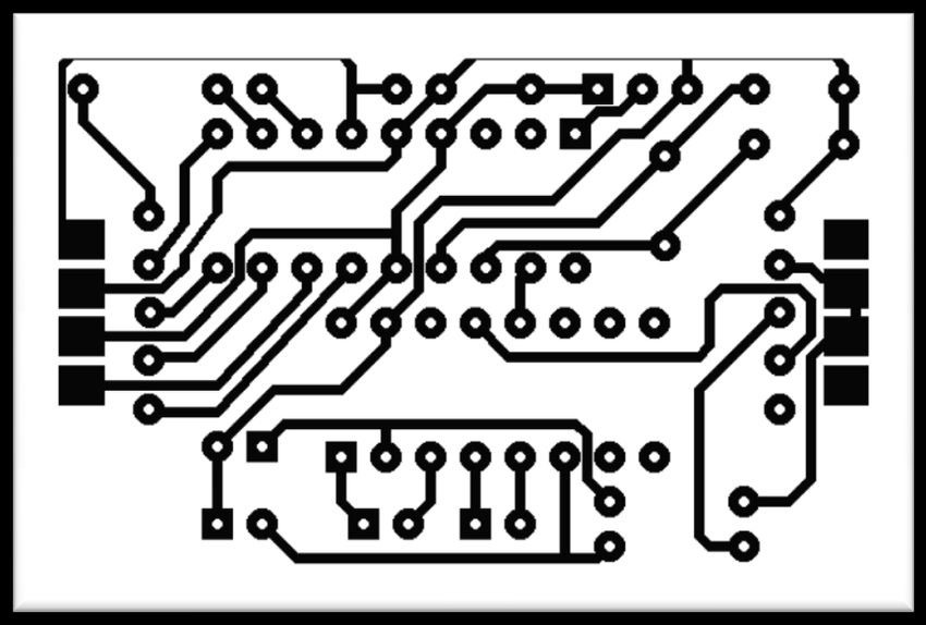
A Printed Circuit Board, or PCB, is a board used to connect electronic components together. They are found in everything from computers to cell phones to calculators. PCBs can be simple, with only a few components, or they can be very complex, with hundreds of components. The diagram of a PCB shows how the components are connected together.
PCB Design
PCB design is the process of creating a printed circuit board. A PCB is made up of a series of copper tracks on a insulating board. These tracks are used to connect electronic components together. The design of a PCB is important as it determines how well the board will function.
There are a few things to consider when designing a PCB. The first is the width of the tracks. This needs to be wide enough to carry the current from the component to the next. The second is the spacing between tracks. This needs to be small enough so that the tracks do not short out. The third is the size of the board. This needs to be large enough to fit all the components.
Designing a PCB can be done by hand or using software. When using software, it is important to use a program that can generate a gerber file. This file can be sent to a PCB manufacturer to have the board made.
PCB Layout
PCB layout is the process of arranging the various components on a printed circuit board so that they function properly. This includes placing the components in the correct positions, routing the traces between them, and creating the necessary vias and pads.
PCB layout is a critical part of the design process, as it can have a significant impact on the performance of the finished product. Poorly designed PCBs can be unreliable and difficult to manufacture, so it is important to get it right.
When designing a PCB layout, there are a number of factors to consider, such as the size and shape of the board, the spacing between components, and the routing of the traces. The layout must also take into account the power and signal requirements of the components.
Once the layout is complete, it must be checked for errors and potential problems. This includes ensuring that all the traces are properly connected and that there are no shorts or open circuits. The layout can then be sent to a fabrication shop for manufacturing.
PCB Fabrication
PCB fabrication is the process of making a printed circuit board. This can be done by etching a copperclad board, or by using a pre-made PCB. The PCB is made up of conductive tracks, which are etched onto a non-conductive substrate. The tracks are then coated with a thin layer of copper, which is then etched away to leave the desired pattern.
PCB Assembly
PCB Assembly is the process of soldering electronic components to a printed circuit board (PCB) to create an electronic device. The assembly process begins with a PCB design, which is created using computer-aided design (CAD) software. Once the design is complete, the PCB is sent to a fabrication plant where it is manufactured. Once the PCB is manufactured, it is sent to an assembly plant where electronic components are soldered to the board. The assembly process is completed by testing the device to ensure it is functioning properly.
PCB Rework
A Printed Circuit Board, or PCB, is a board used to connect electronic components together. They are typically made of a thin layer of copper or other conductive material sandwiched between two insulating layers.
PCBs are used in a variety of electronic devices, from simple circuits to more complex ones found in computers and other digital devices. In order to function properly, each component must be properly connected to the PCB. This can be done using either through-hole or surface-mount technology.
Through-hole technology involves passing component leads through holes in the PCB and then soldering them in place on the other side. Surface-mount technology, on the other hand, involves soldering components to pads on the surface of the PCB.
PCB Rework is the process of modifying a PCB after it has been fabricated. This can be necessary for a variety of reasons, such as fixing errors, adding or removing components, or making changes to the design.
Rework can be a complex and time-consuming process, so it is important to have a clear understanding of what needs to be done before starting. In some cases, it may be necessary to remove and replace entire sections of the PCB. In others, only small changes may be required.
Once the necessary changes have been made, the PCB can then be tested to ensure that it is functioning properly.
PCB Repair
A printed circuit board (PCB) is a board that connects electronic components together. It is made of a special material called substrate, which is usually made of fiberglass or another type of material. The substrate has conductive pathways etched into it that connect the different components.
PCBs are used in a variety of electronic devices, from computers and cell phones to televisions and radios. They are an essential part of how these devices work.
When a PCB needs to be repaired, it is usually because one of the components has failed. The first step is to identify the failed component. This can be done by using a multimeter to test the continuity of the different pathways. Once the failed component is identified, it can be replaced.
PCB repairs can be simple or complex, depending on the nature of the problem. In some cases, only a single component needs to be replaced. In other cases, the entire board may need to be replaced.
PCB repairs are best done by experienced professionals. However, with the right tools and instructions, they can be done by anyone.
PCB EMC Compliance
PCB EMC compliance is a sub section of the main topic, printed circuit board diagram. This compliance involves making sure that the PCB design meets the requirements for electromagnetic compatibility. There are many factors that go into ensuring PCB EMC compliance, such as the material used for the PCB, the layout of the PCB, and the way the PCB is manufactured.
PCB EMC Testing
EMC testing is a process of testing a printed circuit board (PCB) to ensure that it meets the requirements for electromagnetic compatibility (EMC). The goal of EMC testing is to ensure that the PCB does not emit electromagnetic interference (EMI) that can interfere with the operation of other electronic devices. EMC testing is typically done by measuring the emissions of the PCB with an electromagnetic compatibility (EMC) test receiver. The emissions of the PCB are then compared to the emissions limits for the intended environment in which the PCB will be used. If the emissions of the PCB exceed the emissions limits, the PCB must be redesigned to reduce the emissions.
PCB Design Software
There are many different software packages available for designing printed circuit boards (PCBs), and the choice of which to use can be quite overwhelming for someone just starting out. Some packages are free, while others cost hundreds or even thousands of dollars. Some are very simple and easy to use, while others are much more complex and require a significant learning curve.
The most important thing to consider when choosing a PCB design software package is what level of complexity you need. If you are just designing simple boards with a few components, then a free or low-cost package may be all you need. If you are planning on designing more complex boards with a large number of components, then you will need a more powerful and expensive package.
Once you have decided on the level of complexity you need, you can then start looking at specific software packages. There are many reviews and comparisons of different PCB design software packages available online, so you should be able to find one that meets your needs.